What is MPW & Why is it Critical?

A Multi-Project Wafer (MPW) service, often called a "shuttle," combines multiple distinct chip designs onto shared silicon wafers. This aggregation allows numerous projects to share the immense mask and fabrication costs, making silicon prototyping economically feasible.
Cost Barrier Demolition: Full mask sets cost millions ($1M+ for 28nm, $10M+ for 7nm). MPWs can reduce prototyping NRE (Non-Recurring Engineering) costs by up to 90%. Instead of funding a full production run, startups purchase a small "seat" on a shared wafer run.
Risk Reduction & Faster Iteration: Testing real silicon early is invaluable for finding bugs missed in simulation. MPWs allow for hardware validation before committing to high-volume production masks. If a design flaw requires a respin, the financial hit is dramatically lower with an MPW compared to a full mask set.
The Startup Enabler: Since the 1980s, MPW services (like MOSIS, Europractice, CMP, and foundry programs like TSMC CyberShuttle) have been fundamental to hardware innovation, particularly for budget-constrained startups and academic research. Often, it's the only practical way to get custom silicon manufactured early in a company's lifecycle.
Premium Tools & Insights Hub
Go beyond basic info. Leverage actionable calculators, up-to-date schedules*, readiness scorecards, practical templates, and hard-won lessons to de-risk your tapeout and accelerate time-to-silicon.
Realistic MPW Planning Calculators
Get instant estimates tailored to your project. Refine your budget and timeline with data-driven insights. (Note: Benchmarks are illustrative.)
Enhanced Cost Estimator
Time-to-Silicon Estimator
Yield vs. Buffer Planner
Aggregated MPW Shuttle Schedule (Illustrative)
Stop hunting across fragmented sites. Get a centralized view of upcoming deadlines. (Note: Live data requires premium subscription. Below is static demo data based on typical patterns.)
| Foundry/Broker | Process Node | Tapeout Deadline | Est. Delivery | Status | Notes |
|---|---|---|---|---|---|
| Europractice | TSMC 65nm LPe | May 15, 2025 | Aug 20, 2025 | Closing Soon | Standard CMOS |
| TSMC CyberShuttle | TSMC 28nm HPC+ | May 30, 2025 | Sep 15, 2025 | Open | High Performance |
| Europractice | TSMC 16FFC | Jun 10, 2025 | Oct 15, 2025 | Open | FinFET, Check Rules |
| GF GlobalShuttle | GF 130nm SiGe | Jun 20, 2025 | Sep 25, 2025 | Open | RF/Analog Focus |
| TSMC CyberShuttle | TSMC 65nm LP | Jun 30, 2025 | Sep 30, 2025 | Open | Low Power |
| Europractice | XFAB 180nm XH018 | Jul 05, 2025 | Oct 01, 2025 | Open | Mixed-Signal/HV |
| Europractice | UMC 40nm LP | Apr 30, 2025 | Jul 30, 2025 | Closed | - |
*Schedule data is illustrative and may not be accurate. Always confirm directly with providers.
Illustrative MPW Pricing Examples
Get a feel for typical MPW seat costs. Prices vary significantly based on provider, node, area, options, and volume discounts. (Note: These are estimates based on public data and typical ranges. Obtain official quotes.)
| Foundry | Process Node | Min. Block Size | Est. Price (USD) | Notes |
|---|---|---|---|---|
| X-Fab | 180nm XH018 | ~5 mm² | ~$20,000 - $30,000 | Good for Analog/HV |
| TSMC | 130nm MS/RF | ~5 mm² | ~$30,000 - $45,000 | Via Broker/Direct |
| TSMC / UMC | 65nm LP/LPe | ~4 mm² | ~$50,000 - $75,000 | Via Broker/Direct |
| TSMC / UMC | 40nm LP | ~3-4 mm² | ~$80,000 - $120,000 | Via Broker/Direct |
| TSMC | 28nm HPC/HPC+ | ~2 mm² | ~$100,000 - $160,000+ | Via Broker/Direct |
| GlobalFoundries | 22FDX (FD-SOI) | ~2 mm² | ~$180,000 - $250,000+ | Specialty Low Power/RF |
| TSMC | 16nm FFC/FF+ | ~1-2 mm² | ~$200,000 - $400,000+ | FinFET, High Cost/Complexity |
*Prices are highly illustrative, exclude packaging/IP/EDA, and depend heavily on exact options and provider agreements. Use the Cost Considerations section and Budget Template for detailed planning.
Foundry/Node Readiness Scorecards
Don't choose blindly. Quickly assess the suitability of common MPW options for startups based on PDK access, IP availability, tool complexity, and first-timer risk.
Mid-Range Node (e.g., 65nm)
Advanced Planar (e.g., 28nm)
Early FinFET (e.g., 16/14nm)
Templates & Downloads
Save hours with ready-to-use templates and examples for critical MPW tasks and documentation. View previews below or copy/download source files.
Minimal Bring-up PCB Schematic

Reference design including power, clock, JTAG, IO breakout, and UART.
Download Schematic (PNG)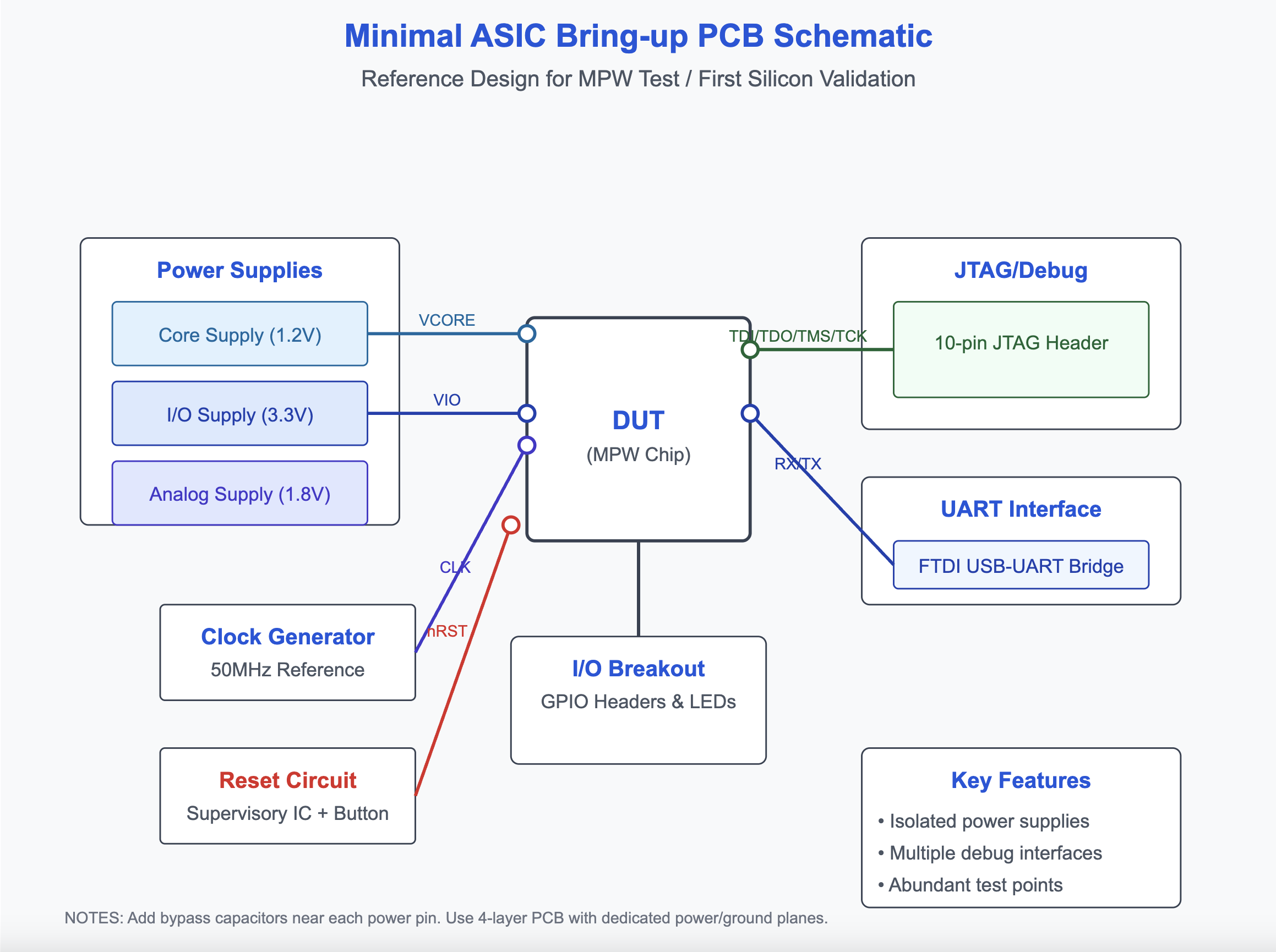
Bonding Diagram Template

Standard format for specifying die pads and package connections.
Download Bonding Diagram (PNG)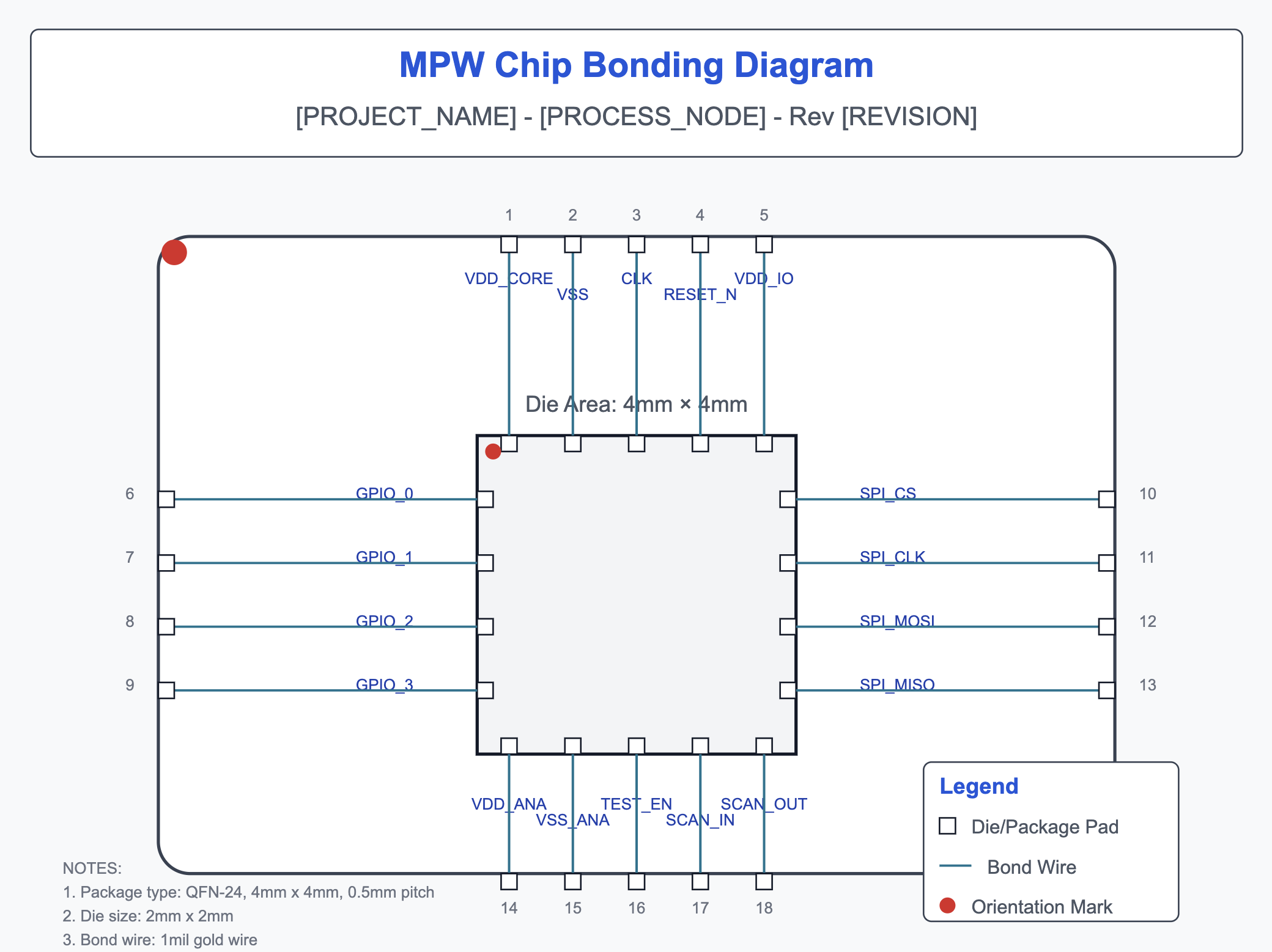
First Test Scripts (Python Example)
#!/usr/bin/env python3
"""
# MPW First Silicon Validation Framework
# =====================================
#
# STARTUP GUIDE: This script provides a systematic approach to validate your first silicon from
# an MPW (Multi-Project Wafer) shuttle run. It's designed to be beginner-friendly while still
# being comprehensive enough for professional use.
#
# KEY CONCEPTS:
# - Power sequencing: Ensures proper voltage application to prevent latch-up/damage
# - Current monitoring: Detects shorts and excessive power consumption
# - Basic connectivity: Validates that fundamental interfaces (JTAG, GPIO) are operational
# - Functional tests: Checks basic chip functionality (clocks, memory, etc.)
#
# SETUP REQUIREMENTS:
# 1. Test fixture with power supplies, JTAG adapter, and GPIO pins connected to chip
# 2. Python 3.6+ with numpy and logging modules
# 3. Appropriate equipment drivers (edit the Equipment Interface Wrappers section)
#
# CUSTOMIZATION:
# - Update expected current values in power_up_sequence() based on your design
# - Modify JTAG ID code in jtag_basic_test() to match your chip
# - Add additional functional tests specific to your design
"""

import time
import logging
import numpy as np
from datetime import datetime
import os
import json
import sys

# =========================================================================
# CONFIGURATION - EDIT THESE SETTINGS TO MATCH YOUR CHIP AND TEST SETUP
# =========================================================================

# Chip-specific constants - MODIFY THESE FOR YOUR DESIGN
CHIP_NAME = "YOUR_CHIP_NAME"  # Replace with your chip's name
EXPECTED_JTAG_ID = 0x12345678  # Replace with your chip's expected JTAG ID code

# Power supply configuration - MODIFY THESE FOR YOUR DESIGN
POWER_RAILS = {
    "VCORE": {"nominal_voltage": 1.2, "max_current": 0.05, "min_current": 0.001},
    "VIO": {"nominal_voltage": 3.3, "max_current": 0.02, "min_current": 0.001},
    "VANA": {"nominal_voltage": 1.8, "max_current": 0.01, "min_current": 0.001}
}

# GPIO pin mapping - MODIFY THESE FOR YOUR TEST SETUP
GPIO_PINS = {
    "CLK_MON": 5,    # Pin connected to clock monitor output
    "BIST_EN": 6,    # Pin to enable memory BIST
    "BIST_DONE": 7,  # Pin that signals BIST completion
    "BIST_PASS": 8   # Pin that signals BIST pass/fail result
}

# JTAG configuration - MODIFY THESE FOR YOUR TEST SETUP
JTAG_CONFIG = {
    "adapter_type": "ftdi",  # Options: "ftdi", "jlink", "buspirate", etc.
    "serial": None,          # Serial number of adapter (if multiple connected)
    "interface": "jtag",     # Options: "jtag", "swd"
    "speed": 1000            # Clock speed in kHz
}

# =========================================================================
# LOGGING SETUP
# =========================================================================

# Create a results directory if it doesn't exist
results_dir = "test_results"
if not os.path.exists(results_dir):
    os.makedirs(results_dir)

# Set up logging to both console and file
test_time = datetime.now().strftime("%Y%m%d_%H%M%S")
log_filename = os.path.join(results_dir, f"chip_test_{test_time}.log")

logging.basicConfig(
    level=logging.INFO,
    format='%(asctime)s - %(levelname)s - %(message)s',
    handlers=[
        logging.FileHandler(log_filename),
        logging.StreamHandler()
    ]
)

# =========================================================================
# EQUIPMENT INTERFACE WRAPPERS
# =========================================================================
# NOTE: These functions provide a common interface for different test equipment.
# You'll need to replace the placeholder code with actual commands for your hardware.
# Common equipment interfaces include PyVISA for GPIB/USB instruments and PySerial for UART.

def power_supply_set_voltage(rail, voltage, current_limit=None):
    """
    Set voltage on specified power rail with current limit

    Parameters:
    - rail (str): Name of the power rail
    - voltage (float): Voltage in Volts
    - current_limit (float): Current limit in Amps

    Returns:
    - bool: True if successful, False otherwise

    Implementation Tips:
    - For Keysight/Agilent: pyvisa.ResourceManager().open_resource("GPIB::5::INSTR").write(f"VOLT {voltage}")
    - For Keithley: pyvisa.ResourceManager().open_resource("GPIB::24::INSTR").write(f"SOUR:VOLT {voltage}")
    """
    if current_limit is None and rail in POWER_RAILS:
        current_limit = POWER_RAILS[rail]["max_current"] * 1.2  # 20% margin

    logging.info(f"Setting {rail} to {voltage:.3f}V (limit: {current_limit:.3f}A)")

    # TODO: Replace with your actual hardware communication code
    # This is a placeholder for simulation
    try:
        # Simulate communication with power supply
        # Your actual code would communicate with your power supply here
        return True
    except Exception as e:
        logging.error(f"Failed to set {rail} voltage: {str(e)}")
        return False

def power_supply_enable(rail):
    """
    Enable the specified power rail

    Implementation Tips:
    - Some supplies need an OUTPUT ON command
    - Some supplies enable when voltage is set
    """
    logging.info(f"Enabling {rail}")

    # TODO: Replace with your actual hardware communication code
    # This is a placeholder for simulation
    try:
        # Your actual code would communicate with your power supply here
        return True
    except Exception as e:
        logging.error(f"Failed to enable {rail}: {str(e)}")
        return False

def power_supply_disable(rail):
    """Disable the specified power rail"""
    logging.info(f"Disabling {rail}")

    # TODO: Replace with your actual hardware communication code
    return True

def measure_current(rail):
    """
    Measure current on the specified rail

    Implementation Tips:
    - For Keysight/Agilent: float(pyvisa.ResourceManager().open_resource("GPIB::5::INSTR").query("MEAS:CURR?"))
    - For Keithley: float(pyvisa.ResourceManager().open_resource("GPIB::24::INSTR").query("MEAS:CURR?"))
    """
    # TODO: Replace with your actual hardware communication code
    # This is a placeholder for simulation
    try:
        # Simulate current measurement
        # For demonstration purposes, we'll return a random value within expected range
        import random
        if rail in POWER_RAILS:
            min_current = POWER_RAILS[rail]["min_current"]
            max_current = POWER_RAILS[rail]["max_current"]
            current = random.uniform(min_current, max_current)
        else:
            current = random.uniform(0.001, 0.1)  # Default 1-100mA

        logging.info(f"Measured {rail} current: {current*1000:.2f} mA")
        return current
    except Exception as e:
        logging.error(f"Failed to measure {rail} current: {str(e)}")
        return None

def jtag_connect(config=None):
    """
    Initialize JTAG connection

    Implementation Tips:
    - For OpenOCD: subprocess.run(["openocd", "-f", "interface/ftdi/digilent-hs1.cfg", "-f", "target/your_chip.cfg"])
    - For PyFtdi: from pyftdi.jtag import JtagEngine; jtag = JtagEngine(); jtag.configure("ftdi://ftdi:2232h/1")
    """
    if config is None:
        config = JTAG_CONFIG

    logging.info(f"Initializing JTAG with {config['adapter_type']} adapter")

    # TODO: Replace with your actual JTAG initialization code
    # This is a placeholder for simulation
    try:
        # Your actual code would initialize JTAG here
        return True
    except Exception as e:
        logging.error(f"Failed to connect to JTAG: {str(e)}")
        return False

def jtag_scan():
    """
    Scan JTAG chain for devices

    Returns:
    - list: List of detected devices with their IDCODE
    """
    logging.info("Scanning JTAG chain for devices")

    # TODO: Replace with your actual JTAG scanning code
    # This is a placeholder for simulation
    try:
        # Simulate finding the chip on the JTAG chain
        return [f"{CHIP_NAME} (IDCODE: 0x{EXPECTED_JTAG_ID:08X})"]
    except Exception as e:
        logging.error(f"Failed to scan JTAG chain: {str(e)}")
        return []

def jtag_read_id():
    """
    Read JTAG IDCODE from the device

    Returns:
    - int: JTAG IDCODE
    """
    logging.info("Reading JTAG IDCODE")

    # TODO: Replace with your actual JTAG ID reading code
    # This is a placeholder for simulation
    try:
        # Simulate reading the JTAG ID
        return EXPECTED_JTAG_ID
    except Exception as e:
        logging.error(f"Failed to read JTAG ID: {str(e)}")
        return None

def uart_configure(port, baudrate=115200):
    """
    Configure UART connection

    Implementation Tips:
    - Using PySerial: import serial; ser = serial.Serial('/dev/ttyUSB0', 115200)
    """
    logging.info(f"Configuring UART on {port} at {baudrate} baud")

    # TODO: Replace with your actual UART configuration code
    # This is a placeholder for simulation
    try:
        # Your actual code would configure the UART here
        return True
    except Exception as e:
        logging.error(f"Failed to configure UART: {str(e)}")
        return False

def gpio_configure(pin_name, direction="input"):
    """
    Configure GPIO pin direction

    Implementation Tips:
    - Using RPi.GPIO: import RPi.GPIO as GPIO; GPIO.setup(pin, GPIO.IN if direction=="input" else GPIO.OUT)
    - Using PyFtdi: from pyftdi.gpio import GpioController; gpio = GpioController(); gpio.configure(pin, direction)
    """
    if pin_name in GPIO_PINS:
        pin = GPIO_PINS[pin_name]
    else:
        pin = pin_name  # Assume direct pin number if not in mapping

    logging.info(f"Configuring GPIO pin {pin_name} (#{pin}) as {direction}")

    # TODO: Replace with your actual GPIO configuration code
    # This is a placeholder for simulation
    try:
        # Your actual code would configure the GPIO here
        return True
    except Exception as e:
        logging.error(f"Failed to configure GPIO pin {pin_name}: {str(e)}")
        return False

def gpio_set(pin_name, value):
    """Set GPIO pin output value"""
    if pin_name in GPIO_PINS:
        pin = GPIO_PINS[pin_name]
    else:
        pin = pin_name  # Assume direct pin number if not in mapping

    logging.info(f"Setting GPIO pin {pin_name} (#{pin}) to {value}")

    # TODO: Replace with your actual GPIO write code
    # This is a placeholder for simulation
    try:
        # Your actual code would set the GPIO here
        return True
    except Exception as e:
        logging.error(f"Failed to set GPIO pin {pin_name}: {str(e)}")
        return False

def gpio_read(pin_name):
    """Read GPIO pin input value"""
    if pin_name in GPIO_PINS:
        pin = GPIO_PINS[pin_name]
    else:
        pin = pin_name  # Assume direct pin number if not in mapping

    # TODO: Replace with your actual GPIO read code
    # This is a placeholder for simulation
    try:
        # Simulate reading a GPIO pin
        # For demonstration, we'll randomize but bias toward 1
        import random
        value = 1 if random.random() > 0.2 else 0
        logging.info(f"Read GPIO pin {pin_name} (#{pin}): {value}")
        return value
    except Exception as e:
        logging.error(f"Failed to read GPIO pin {pin_name}: {str(e)}")
        return None

# =========================================================================
# TEST SEQUENCES
# =========================================================================

def power_up_sequence():
    """
    Basic power-up sequence for initial chip testing

    Purpose:
    - Safe power-up of the chip to avoid damage
    - Basic current measurement to detect shorts/issues
    - Go/no-go check for proceeding with further testing

    Returns:
    - bool: True if successful, False otherwise
    - dict: Measurement data
    """
    logging.info("===== STARTING POWER-UP SEQUENCE =====")

    # Data structure to store measurements for reporting
    measurements = {
        "timestamp": datetime.now().isoformat(),
        "currents": {},
        "voltages": {},
        "pass": False
    }

    # Define power-up order (typically core voltage first, then I/O, then analog)
    rail_sequence = ["VCORE", "VIO", "VANA"]

    # First, ensure all supplies are at 0V
    for rail in rail_sequence:
        power_supply_set_voltage(rail, 0.0)
        power_supply_enable(rail)
        measurements["voltages"][rail] = 0.0

    # Power up each rail in sequence
    for rail in rail_sequence:
        target_voltage = POWER_RAILS[rail]["nominal_voltage"]
        max_current = POWER_RAILS[rail]["max_current"]
        min_current = POWER_RAILS[rail]["min_current"]

        logging.info(f"Ramping {rail} to {target_voltage}V...")

        # Optional: For sensitive chips, ramp voltage gradually
        # for v in np.linspace(0, target_voltage, 5):
        #     power_supply_set_voltage(rail, v)
        #     time.sleep(0.05)

        power_supply_set_voltage(rail, target_voltage)
        time.sleep(0.1)  # Allow current to stabilize

        # Measure and check current
        current = measure_current(rail)
        if current is None:
            logging.error(f"Failed to measure {rail} current. Aborting power-up!")
            power_supply_disable(rail)
            return False, measurements

        measurements["currents"][rail] = current
        measurements["voltages"][rail] = target_voltage

        # Check for overcurrent condition
        if current > max_current:
            logging.error(f"{rail} current too high: {current*1000:.2f} mA (limit: {max_current*1000:.2f} mA). Aborting power-up!")
            power_supply_disable(rail)
            return False, measurements

        # Check for undercurrent - might indicate open circuit
        if current < min_current:
            logging.warning(f"{rail} current suspiciously low: {current*1000:.2f} mA (expected: >{min_current*1000:.2f} mA)")
            # Continue but flag warning

    # Log all power measurements
    logging.info("Power-up currents:")
    for rail, current in measurements["currents"].items():
        logging.info(f"  {rail}: {current*1000:.2f} mA (limit: {POWER_RAILS[rail]['max_current']*1000:.2f} mA)")

    # Check if all rails are within expected ranges
    all_currents_ok = all(
        POWER_RAILS[rail]["min_current"] <= measurements["currents"].get(rail, 0) <= POWER_RAILS[rail]["max_current"]
        for rail in rail_sequence
    )

    if all_currents_ok:
        logging.info("Power-up sequence completed successfully. All currents within expected ranges.")
        measurements["pass"] = True
        return True, measurements
    else:
        logging.warning("Power-up completed but some currents outside expected ranges. Proceed with caution.")
        return True, measurements

def jtag_basic_test():
    """
    Basic JTAG connectivity test

    Purpose:
    - Verify JTAG connection to the chip
    - Confirm correct chip ID
    - Basic test of boundary scan functionality

    Returns:
    - bool: True if successful, False otherwise
    - dict: Test data
    """
    logging.info("===== STARTING BASIC JTAG CONNECTIVITY TEST =====")

    results = {
        "timestamp": datetime.now().isoformat(),
        "detected_devices": [],
        "idcode": None,
        "idcode_match": False,
        "pass": False
    }

    # Connect to JTAG adapter
    if not jtag_connect():
        logging.error("Failed to connect to JTAG adapter!")
        return False, results

    # Scan for devices on the JTAG chain
    devices = jtag_scan()
    results["detected_devices"] = devices

    logging.info(f"Detected JTAG devices: {devices}")
    if not devices:
        logging.error("No devices detected on JTAG chain!")
        return False, results

    # Read IDCODE and verify it matches expected value
    id_code = jtag_read_id()
    results["idcode"] = id_code

    if id_code is None:
        logging.error("Failed to read JTAG IDCODE!")
        return False, results

    logging.info(f"Read IDCODE: 0x{id_code:08X}")

    expected_id = EXPECTED_JTAG_ID
    results["idcode_match"] = (id_code == expected_id)

    if id_code == expected_id:
        logging.info("JTAG ID code matches expected value!")
        results["pass"] = True
        return True, results
    else:
        logging.error(f"JTAG ID code mismatch! Expected 0x{expected_id:08X}, got 0x{id_code:08X}")
        return False, results

def clock_verification():
    """
    Verify that clock is running by checking a clock monitor output pin

    Purpose:
    - Confirm oscillator/PLL is running
    - Verify clock monitor circuit is working

    Implementation Notes:
    - Assumes the chip has a clock monitor output pin that toggles when clock is running
    - For more detailed analysis, connect to a frequency counter or oscilloscope

    Returns:
    - bool: True if successful, False otherwise
    - dict: Test data
    """
    logging.info("===== CHECKING CLOCK MONITOR OUTPUT =====")

    results = {
        "timestamp": datetime.now().isoformat(),
        "readings": [],
        "toggling": False,
        "pass": False
    }

    gpio_configure("CLK_MON", "input")

    # Take several readings to see if the pin is toggling
    logging.info("Sampling clock monitor pin...")
    for i in range(10):
        reading = gpio_read("CLK_MON")
        if reading is not None:
            results["readings"].append(reading)
        time.sleep(0.01)

    # If the pin toggles at least once, clock is likely running
    if len(set(results["readings"])) > 1:
        logging.info("Clock monitor pin is toggling - clock appears to be running")
        results["toggling"] = True
        results["pass"] = True
        return True, results
    else:
        logging.error("Clock monitor pin is static - clock may not be running")
        return False, results

def memory_bist_test():
    """
    Run Built-In Self Test for on-chip memories

    Purpose:
    - Validate memory functionality
    - Check for manufacturing defects

    Implementation Notes:
    - Assumes the chip has a BIST engine controlled by GPIO pins
    - Customize this according to your specific BIST implementation

    Returns:
    - bool: True if successful, False otherwise
    - dict: Test data
    """
    logging.info("===== STARTING MEMORY BIST TEST =====")

    results = {
        "timestamp": datetime.now().isoformat(),
        "timeout": False,
        "bist_done": False,
        "bist_pass": False,
        "pass": False
    }

    # Configure control and status pins
    gpio_configure("BIST_EN", "output")
    gpio_configure("BIST_DONE", "input")
    gpio_configure("BIST_PASS", "input")

    # Start BIST by pulsing enable pin
    logging.info("Triggering memory BIST...")
    gpio_set("BIST_EN", 1)
    time.sleep(0.1)
    gpio_set("BIST_EN", 0)

    # Wait for BIST to complete with timeout
    logging.info("Waiting for BIST completion...")
    start_time = time.time()
    timeout = 5.0  # 5 second timeout

    while not gpio_read("BIST_DONE"):
        if time.time() - start_time > timeout:
            logging.error(f"Memory BIST timeout after {timeout} seconds - no completion signal detected")
            results["timeout"] = True
            return False, results
        time.sleep(0.1)

    results["bist_done"] = True

    # Check BIST result
    bist_pass = gpio_read("BIST_PASS")
    results["bist_pass"] = bist_pass

    if bist_pass:
        logging.info("Memory BIST PASSED")
        results["pass"] = True
        return True, results
    else:
        logging.error("Memory BIST FAILED")
        return False, results

def run_all_tests():
    """
    Run complete initial test suite

    Purpose:
    - Structured verification of all chip functionality
    - Collects results for analysis and reporting

    Returns:
    - dict: Results for all tests
    """
    logging.info("\n")
    logging.info("=" * 80)
    logging.info("===== STARTING COMPLETE TEST SUITE =====")
    logging.info("=" * 80)

    all_results = {
        "chip_name": CHIP_NAME,
        "timestamp": datetime.now().isoformat(),
        "tests": {},
        "overall_pass": False
    }

    # Power up the chip
    power_result, power_data = power_up_sequence()
    all_results["tests"]["power_up"] = {
        "pass": power_result,
        "data": power_data
    }

    # If power-up failed, abort further tests
    if not power_result:
        logging.error("Power-up failed! Aborting further tests.")
        return all_results

    # JTAG connectivity test
    jtag_result, jtag_data = jtag_basic_test()
    all_results["tests"]["jtag_test"] = {
        "pass": jtag_result,
        "data": jtag_data
    }

    # Clock verification
    clock_result, clock_data = clock_verification()
    all_results["tests"]["clock_test"] = {
        "pass": clock_result,
        "data": clock_data
    }

    # Only run memory BIST if JTAG and clock are working
    if jtag_result and clock_result:
        mem_result, mem_data = memory_bist_test()
        all_results["tests"]["memory_test"] = {
            "pass": mem_result,
            "data": mem_data
        }

    # Add custom tests here
    # Example:
    # if conditions_met:
    #     custom_result, custom_data = your_custom_test()
    #     all_results["tests"]["custom_test"] = {
    #         "pass": custom_result,
    #         "data": custom_data
    #     }

    # Calculate overall pass/fail status
    all_tests_passed = all(
        test_info["pass"] for test_info in all_results["tests"].values()
    )
    all_results["overall_pass"] = all_tests_passed

    # Print summary
    logging.info("\n")
    logging.info("=" * 80)
    logging.info("===== TEST RESULTS SUMMARY =====")
    logging.info("=" * 80)

    for test, result in all_results["tests"].items():
        status = "PASS" if result["pass"] else "FAIL"
        logging.info(f"{test}: {status}")

    overall_status = "PASS" if all_results["overall_pass"] else "FAIL"
    logging.info(f"Overall result: {overall_status}")

    # Save results to JSON file
    results_file = os.path.join(results_dir, f"chip_test_results_{test_time}.json")
    with open(results_file, 'w') as f:
        json.dump(all_results, f, indent=2)

    logging.info(f"Detailed results saved to: {results_file}")

    return all_results

# =========================================================================
# CUSTOM TESTS - ADD YOUR OWN TESTS HERE
# =========================================================================

def custom_test_template():
    """
    Template for creating custom tests

    Purpose:
    - [Describe what this test verifies]

    Implementation Notes:
    - [Any important details about the test procedure]

    Returns:
    - bool: True if successful, False otherwise
    - dict: Test data
    """
    logging.info("===== STARTING CUSTOM TEST =====")

    results = {
        "timestamp": datetime.now().isoformat(),
        # Add test-specific data here
        "pass": False
    }

    # Your test implementation here
    # ...

    # Example:
    # if everything_passed:
    #     logging.info("Custom test PASSED")
    #     results["pass"] = True
    #     return True, results
    # else:
    #     logging.error("Custom test FAILED")
    #     return False, results

    # Placeholder return
    return False, results

# =========================================================================
# MAIN TEST EXECUTION
# =========================================================================

def print_help():
    """Display usage information"""
    print("\nMPW First Silicon Test Script")
    print("-----------------------------")
    print("Usage: python chip_test.py [command]")
    print("\nCommands:")
    print("  help         - Show this help")
    print("  power        - Run power-up sequence only")
    print("  jtag         - Run JTAG test only")
    print("  clock        - Run clock verification only")
    print("  memory       - Run memory BIST test only")
    print("  run          - Run all tests")
    print("  interactive  - Run interactive test session")
    print("\nExample: python chip_test.py run")

def interactive_mode():
    """Interactive test session"""
    print("\n===== INTERACTIVE TEST SESSION =====")
    print("Enter 'q' or 'quit' to exit")

    while True:
        print("\nAvailable tests:")
        print("1. Power-up sequence")
        print("2. JTAG test")
        print("3. Clock verification")
        print("4. Memory BIST")
        print("5. Run all tests")
        print("q. Quit")

        choice = input("\nEnter selection: ")

        if choice.lower() in ('q', 'quit'):
            break
        elif choice == '1':
            power_up_sequence()
        elif choice == '2':
            jtag_basic_test()
        elif choice == '3':
            clock_verification()
        elif choice == '4':
            memory_bist_test()
        elif choice == '5':
            run_all_tests()
        else:
            print("Invalid selection")

if __name__ == "__main__":
    logging.info("=" * 80)
    logging.info(f"===== MPW FIRST SILICON TEST SCRIPT - {CHIP_NAME} =====")
    logging.info("=" * 80)
    logging.info(f"Test started at: {datetime.now().strftime('%Y-%m-%d %H:%M:%S')}")

    # Process command line arguments
    if len(sys.argv) > 1:
        command = sys.argv[1].lower()
        if command == 'power':
            power_up_sequence()
        elif command == 'jtag':
            jtag_basic_test()
        elif command == 'clock':
            clock_verification()
        elif command == 'memory':
            memory_bist_test()
        elif command == 'run':
            run_all_tests()
        elif command == 'interactive':
            interactive_mode()
        elif command in ('help', '-h', '--help'):
            print_help()
        else:
            print(f"Unknown command: {command}")
            print_help()
    else:
        # No arguments, show help
        print_help()

    logging.info("=" * 80)
    logging.info("===== TEST SCRIPT COMPLETED =====")
    logging.info("=" * 80)
GDS Submission Package Template
MPW GDS Submission Package
===========================

Project Name: [PROJECT_NAME]
Tapeout Date: [TAPEOUT_DATE]
Submission Deadline: [DEADLINE]
MPW Provider: [PROVIDER_NAME]
Process Node: [PROCESS_NODE]

Directory Structure
-------------------
This package contains the following directory structure:

├── 01_GDS_Files/
│   ├── [CHIP_NAME].gds        # Main GDS file (DRC/LVS Clean)
│   ├── [CHIP_NAME].oasis      # Optional OASIS format if required
│   └── cell_library/          # Any custom cell libraries not in PDK
│
├── 02_Documentation/
│   ├── Design_Intent.pdf      # Overall chip description and function
│   ├── Pin_List.csv           # Complete list of pins with function
│   ├── Block_Diagram.pdf      # High-level block diagram
│   └── Special_Requirements.pdf # Any special process/handling needs
│
# ... (rest of README content for preview - truncated for brevity) ...
Standard README structure for GDS submission package, including directory layout, checklist, file info, contacts, etc.
Download Template (.pdf)*PNG/PDF downloads use direct links. Code/Text examples can be copied to clipboard.
Simplified MPW Project Timeline
Visualize the typical phases and dependencies in an MPW project. Use this to plan your resources and milestones.
- Node/Provider Selection
- NDA Execution
- PDK/IP Access
- Tool Setup
- RTL Design
- Simulation
- Layout/P&R
- DRC/LVS/STA
- IP Integration
- Final Checks
- GDS Submission
- Wafer Fabrication
- (Waiting...)
- Dicing
- Packaging
- Test Board Assy
- Bring-up
- Validation
*Durations are highly variable based on design complexity, team experience, and node.
MPW Failure Case Studies & Avoidance
Learn from costly mistakes. These real-world examples highlight critical checks often missed by first-timers. See more detailed examples and prevention strategies on our dedicated page:
Case Study 1: The Forgotten Power Domain
Mistake: A team forgot to connect the power supply for a critical analog block in the top-level layout. LVS passed (schematic matched layout locally), but the block was unpowered.
Actionable Prevention:
- Run full-chip Electrical Rule Checks (ERC) specifically targeting power/ground connectivity for all instances.
- Perform power-aware simulations (e.g., using UPF) if possible.
- Manually trace critical power nets for major blocks during final layout review. Add explicit checklist items for power domain connections.
Case Study 2: The Optimistic Timing Signoff
Mistake: Signed off timing based on typical-typical (TT) process corner only. Silicon came back slow at the slow-slow (SS) corner, failing functional tests at target speed.
Actionable Prevention:
- Mandate STA signoff across all relevant PVT corners specified by the foundry (e.g., SSG, FFG, typical, potentially more).
- Include On-Chip Variation (OCV) / Advanced OCV (AOCV) analysis in timing runs.
- Aim for positive timing margin (e.g., >10% of clock period) on critical paths across all corners, not just zero slack.
Case Study 3: The Misunderstood IP
Mistake: Integrated a third-party memory IP without fully reading the integration guidelines. Missed specific clock gating requirements and boundary signal constraints, leading to memory corruption under specific conditions.
Actionable Prevention:
- Assign dedicated time for thoroughly reading *all* IP documentation (datasheets, integration guides, application notes).
- Run IP vendor-provided example tests and integration checks within your design environment.
- Simulate boundary conditions and specific usage scenarios described in the IP documentation.
- Add IP integration checks (interface protocols, power domains, physical constraints) to your verification plan.
How to Avoid: Pre-Tapeout "Murder Board" Review
Assemble 2-3 experienced engineers (internal or external advisors) unfamiliar with the day-to-day design details. Give them the Tapeout Checklist, key verification reports (DRC, LVS, STA summaries), power analysis, clocking strategy, and IP list 1-2 weeks before tapeout. Their goal: find flaws, question assumptions, and ensure nothing critical was overlooked. Document their findings and required actions.
Beyond the Seat Price: Detailed Cost Considerations
The MPW "seat" price is just the starting point. Use our Budgeting Template to capture these critical cost factors:
Typical Cost Ranges (Illustrative Benchmarks):
- MPW Seat (4-5mm²): Legacy ($15k-$30k), 65nm ($45k-$70k), 28nm ($70k-$130k), FinFET ($180k-$350k+)
- Packaging (50-100 units, QFN): Setup ($3k-$8k) + Per Unit ($8-$20)
- IP (Basic - SRAM/PLL): $10k - $30k (Eval licenses often cheaper)
- EDA Tools (Startup License/Quarter): $15k - $50k+ (Highly variable)
- Test Board Dev & Assy: $5k - $15k
Disclaimer: These are rough estimates. Get specific quotes for your project.
- Base MPW Cost: Quoted price for minimum block size. Price increases non-linearly for larger areas.
- Process Options: Adding layers/features (thick metal, MiM caps) usually incurs extra shared costs.
- Number of Samples: Base price includes fixed dies (e.g., 20-50). More cost extra.
- Packaging & Dicing: Often separate, significant costs. Get quotes early.
- EDA Tool Licenses: Major expense. Look for startup programs.
- IP Licensing: Complex IP requires separate licenses (fees/royalties).
- Engineering Time (NRE): Significant "soft cost" for design, verification, integration.
- Contingency Buffer: Add 15-25% for unexpected issues.
PDK & IP Access: The Nitty-Gritty
Navigating PDK access and IP licensing is critical path. Use our NDA/IP Tracker Template to stay organized.
- NDA Process: Expect weeks for legal review of NDAs with foundries, brokers, and IP vendors. Start early!
- PDK Delivery & Setup: Large downloads requiring specific EDA tool versions and setup procedures. Verify compatibility.
- PDK Contents & Quality: Includes rule decks, models, basic libraries. Quality varies; check documentation/forums for known issues.
- Included vs. Licensed IP: Standard cells/IOs usually included. Memory compilers, complex analog/interface IP (PLLs, SerDes) require separate licenses (often costly).
- IP Integration Challenges: Budget significant time for integrating and verifying third-party IP (interfaces, power, physical views).
- Support Channels: Understand support models (broker vs. foundry vs. IP vendor).
MPW Pre-Tapeout Checklist (Interactive View)
Use this interactive checklist to track your progress towards a successful tapeout. Premium users can also download an editable version.
- All layout objects match schematic objects
- All connections verified
- All device sizes verified
- Final LVS report saved
- All process design rules met
- Minimum width/spacing verified
- Layer density requirements met
- Final DRC report saved
- Parasitics extracted and reviewed
- Post-extraction simulation completed & matches
- IR drop analysis complete & acceptable
- Electromigration rules met
- Timing sign-off across all PVT corners
- Setup/hold times met with margin (>10% recommended)
- Clock skew within limits
- Package submitted to foundry/broker
- Confirmation of receipt obtained
- Local backup of all submission files created
- All required paperwork completed (PO, etc.)
Key Reminders: Keep detailed records. Document all waivers. Start packaging discussions early. Add schedule margin!
After Tapeout: The Post-Fabrication Roadmap
The work isn't over when you submit GDS. Plan these critical post-fab steps using our templates and guides.
- Wafer/Die Delivery & Handling: Know format (wafer, sawn, diced). Use ESD precautions.
- Dicing: If needed, coordinate with a dicing service.
- Packaging Selection & Assembly: Choose package, select OSAT, provide bonding diagrams (use Bonding Diagram Template).
- Test Board Bring-up: Design PCB (use Schematic Template), assemble, perform initial power-on checks.
- Functional Validation: Execute test plan using scripts (see Test Script Examples). Debug issues systematically.
- Failure Analysis (FA): If needed, start with basic electrical checks, then consider advanced FA techniques. Refer to Troubleshooting Guide.
Pro Tip: Design for Testability (DFT) from the start (scan chains, test points). Engage packaging/test partners *before* tapeout.
Ready to Tape Out with Confidence?
Access the complete MPW Premium Toolkit: interactive calculators, live schedules*, readiness scorecards, downloadable templates, detailed case studies, and expert insights to minimize risk and maximize success.
Unlock Premium Toolkit Now*Live schedule updates require premium subscription.