Table of Contents
- Introduction
- Feasibility of Joint Venture (JV) Scenarios
- 2.1. Scenario A: TSMC Operating an Intel Fab
- 2.2. Scenario B: Intel Licensing TSMC Process Technology
- 2.3. Scenario C: Joint Process Node Development
- 2.4. Scenario D: Advanced Packaging Collaboration
- Stakeholder Perspectives
- 3.1. TSMC/Taiwan Perspective
- 3.2. Intel Perspective
- 3.3. U.S. Government Perspective
- 3.4. China’s Potential Reaction
- Broadcom’s Role and Strategic Intentions
- Technical Deep Dive: Comparing TSMC and Intel Technologies
- 5.1. Transistor Architectures & Node Development
- 5.2. Interconnect Materials and Wiring
- 5.3. Lithography & Patterning Methodologies
- 5.4. Advanced Packaging (2.5D and 3D)
- Financial and Market Impact Analysis
- 6.1. Financial Projections Under Different JV Structures
- 6.2. Competitive Impact on Samsung, GlobalFoundries, and Others
- 6.3. Lessons from Past Semiconductor Joint Ventures
- Conclusion
- References
1. Introduction
Rumors of a possible joint venture (JV) between Taiwan Semiconductor Manufacturing Company (TSMC) and Intel have circulated in recent years, fueled by Intel’s efforts to regain process technology leadership and by geopolitical pressures to increase chip manufacturing in the United States. Multiple scenarios have been proposed for a potential JV, ranging from TSMC taking over or operating an Intel fab to Intel licensing TSMC’s process technology, or even co-developing an entirely new process node.
This report evaluates these JV scenarios in detail, explores stakeholder perspectives, examines technical compatibility issues, and assesses financial and market impacts.
2. Feasibility of Joint Venture (JV) Scenarios
Scenario | Key Benefit | Major Challenge | Capex ($B) | Break-even (Years) | |
A | TSMC Operates Intel Fab | Faster yield improvement; potential fabless client attraction | Process incompatibility; Intel loses control | 15 | 6 |
B | Intel Licenses TSMC Node | Lower R&D costs; proven high-yield process | Intel dependent on TSMC’s roadmap; integration issues | 2 | 4 |
C | Joint R&D for Future Node | Cost-sharing on R&D; accelerates technology roadmap | Rival firms sharing IP; risk of roadmap conflicts | 5 | N/A |
D | Advanced Packaging JV | Lower risk; AI & HPC packaging demand growth | Competitive tensions in packaging innovations | 3 | 3 |
2.1. Scenario A: TSMC Operating an Intel Fab
Technical Challenges:
- Process Porting Complexity
- Although both Intel and TSMC use EUV scanners from ASML, their fabs are highly customized, including different photoresists, etch chemistries, and deposition processes, making direct porting infeasible without extensive re-engineering.
- Lithography Differences
- TSMC introduced EUV early at N7+, whereas Intel used complex multi-patterning techniques at 10nm before integrating EUV at Intel 4, complicating alignment in a single fab.
Business Risks:
- Intellectual Property (IP) Risks
- TSMC risks exposing its proprietary yield-enhancing techniques to Intel, eroding its competitive edge.
- Customer Concerns
- Fabless companies like AMD or Nvidia may hesitate to use a TSMC-run fab partially owned by Intel, fearing potential information leaks.
🔴 Conclusion: While the concept makes sense for capacity expansion, the IP risks and technical incompatibilities make this scenario highly unlikely.
2.2. Scenario B: Intel Licensing TSMC Process Technology
Technical Challenges:
- Process Integration Issues
- Intel’s standard cell architectures, transistor designs (FinFET vs. GAA), and interconnect materials (cobalt vs. copper) differ significantly from TSMC’s, requiring years of adaptation.
- Design Migration
- Intel’s x86 CPU architectures are heavily optimized for Intel’s in-house process quirks. Re-designing for TSMC’s PDK (Process Design Kit) would require massive engineering resources.
Business Risks:
- Loss of Control
- Intel becomes dependent on TSMC’s roadmap, contradicting IDM 2.0, which focuses on self-sufficiency.
- Market Confusion
- Customers may prefer going directly to TSMC instead of using Intel as a middleman.
🔴 Conclusion: Licensing a node from a direct competitor is highly unlikely due to control issues and lack of mutual benefit.
2.3. Scenario C: Joint Process Node Development
📋 [Insert: TSMC vs Intel Transistor Technologies Table]
Technical Challenges:
- Different Architectural Philosophies
- Intel’s RibbonFET (GAA) and PowerVia (Backside Power) aim to leapfrog competitors at 18A, while TSMC’s N2 GAA follows an incremental evolution model.
- IP Sharing Risks
- IBM previously sued GlobalFoundries over 7nm abandonment, showcasing the legal risks of joint semiconductor R&D.
Business Risks:
- Competitive Conflict
- Unlike IBM-Samsung partnerships (where IBM was not a volume competitor), Intel and TSMC directly compete in logic foundry business.
🔴 Conclusion: Direct competitors rarely share cutting-edge R&D, making this scenario improbable.
2.4. Scenario D: Advanced Packaging Collaboration
📊 [Insert: Projected Growth of Advanced Packaging Market Line Chart]
Technical Challenges:
- Packaging Design Differences
- Intel’s EMIB and Foveros use small silicon bridges, while TSMC’s CoWoS relies on full silicon interposers. Harmonizing these methods requires careful process alignment.
Business Risks:
- TSMC’s Market Leadership
- TSMC already dominates high-end OSAT (Outsourced Semiconductor Assembly and Test) services; Intel gaining ground could disrupt its position.
✅ Conclusion: This is the most viable JV option, given lower IP risks and strong market demand for AI/HPC chiplet packaging solutions.
Factor | TSMC Strength | Intel Strength | JV Benefit |
Technology | CoWoS – AI packaging leader | EMIB/Foveros – 3D stacking | Combines interposers + stacking |
Performance | Optimized for large AI chips | Efficient for CPU/GPU chips | More powerful & efficient AI/HPC chips |
Integration | Best-in-class interposers | Flexible chiplet integration | Maximizes flexibility & compatibility |
Logistics | Ships wafers from Taiwan | U.S.-based fabs | Reduces cross-Pacific shipments |
Cost | High-volume manufacturing | Leverages in-house chips | Faster, cheaper production |
Market Demand | Dominates AI chip packaging | Expanding U.S. presence | Strengthens leadership in chip packaging |
3. Stakeholder Perspectives
3.1. TSMC/Taiwan Perspective
TSMC’s top priority is protecting its core intellectual property and safeguarding Taiwan’s strategic position as a global leader in leading-edge foundry services. TSMC’s so-called “silicon shield” theoretically deters aggression against Taiwan by making the world reliant on TSMC’s local operations [1][1].
Local media and experts in Taiwan have voiced concern that assisting Intel in the U.S. could undermine Taiwan’s unique leverage if the most advanced fab capabilities shift overseas [1]. TSMC’s leadership repeatedly emphasizes that the most advanced R&D will remain in Taiwan, even as it builds 4 nm or potentially 3 nm fabs in the U.S.
From a purely business standpoint, TSMC does not want to enable a direct competitor to catch up [5]. Past TSMC joint ventures (e.g., with Sony in Japan) have been with customers, not rival foundries. Hence, any JV with Intel would be viewed as high risk and would require ironclad IP protections. Politically, TSMC must also balance U.S. government pressure to expand stateside against Taiwanese sentiment worried about “losing the bowl” of advanced manufacturing to the U.S. [1].
3.2. Intel Perspective
Intel’s “IDM 2.0” strategy, announced under former CEO Pat Gelsinger, aims to regain process technology leadership by 2025–2026 while also attracting external foundry customers. A TSMC partnership could, in theory, accelerate Intel’s ramp and bring in new customers. However, it also threatens Intel’s identity as an integrated device manufacturer that has always prided itself on self-sufficient process leadership [4].
Short-term benefits include improved yields, relief from operational burdens, and possible synergy with TSMC’s extensive customer base [1]. Longer-term, however, Intel risks losing autonomy if it relies on TSMC’s IP or cedes operation of an advanced fab [4]. Culturally, many within Intel would resist adopting TSMC’s processes after decades of internal manufacturing pride. Nonetheless, with Intel’s own efforts running behind schedule—and Gelsinger having departed in late 2024 under pressure [10]—the new leadership might be more open to radical measures.
3.3. U.S. Government Perspective
The U.S. government, underpinned by the CHIPS Act’s $52 billion in semiconductor funding, has strong incentive to bolster domestic manufacturing at the leading edge. A TSMC–Intel JV on U.S. soil could provide a secure, state-of-the-art fab for national security needs [1][1].
However, officials are also wary of ceding any strategic U.S. asset to foreign control. Reports suggest some policymakers would oppose TSMC fully running Intel’s factories, citing national security concerns [11]. Any JV would require navigating export controls, CFIUS reviews, and strings attached to CHIPS Act subsidies. On balance, Washington likely supports a robust onshore fab solution—so long as it preserves sufficient American ownership and IP protections [11].
3.4. China’s Potential Reaction
Beijing would perceive a TSMC–Intel collaboration in the U.S. as further cementing a “chip alliance” designed to exclude China from leading-edge technology [1]. It also diminishes China’s potential leverage in a cross-strait conflict if TSMC’s advanced manufacturing shifts partially to U.S. soil.
China might respond by redoubling efforts to achieve self-sufficiency via SMIC and other domestic foundries. While Beijing could rhetorically protest such a JV, it lacks direct mechanisms to stop it. In the bigger picture, a robust TSMC–Intel JV in America undercuts any notion that China could quickly acquire TSMC’s leading-edge capabilities by pressuring or seizing Taiwan.
4. Broadcom’s Role and Strategic Intentions
Recent reports speculate that Broadcom might seek to purchase Intel’s chip design teams or product lines separately from any TSMC partnership [1][1]. Broadcom is known for an acquisition-centric strategy, focusing on high-margin semiconductor and infrastructure businesses. By acquiring Intel’s design IP (e.g., FPGAs, networking chips), Broadcom could then rely on TSMC or other foundries to manufacture those products—aligning with Broadcom’s fabless model [1].
Such a carve-up would be detrimental to Intel’s foundry ambitions: losing captive product lines to Broadcom would reduce Intel’s internal volume and hamper economies of scale for Intel’s own fabs. If TSMC simultaneously picked up Intel’s manufacturing assets, Intel could be effectively split between design (sold to Broadcom) and manufacturing (transferred to TSMC-led entities), undoing Intel’s traditional IDM model. This scenario underscores the precarious position Intel finds itself in—outside players see value in its design teams more than in its factories, and TSMC might be willing to take over those fabs if the deal is structured favorably [1].
5. Technical Deep Dive: Comparing TSMC and Intel Technologies
5.1. Transistor Architectures & Node Development
| Feature | Intel | TSMC |
|---|---|---|
| Fin Height | Taller Fin (performance-oriented) | Balanced for power & density |
| GAA Transition | RibbonFET (2024, 20A) | Nanosheet GAA (N2, 2025) |
| Power Delivery | Backside Power (PowerVia, 18A) | Front-side Power (initial N2) |
| Process Density | Denser std. cell but lower yield | Higher yield at mass production |
| Primary Customers | High-performance CPUs | Diverse customers (Apple, Nvidia, etc. |
Current FinFET vs. Upcoming GAA
- Intel’s FinFET evolution: Introduced Tri-Gate (FinFET) at 22nm, continuing through 14nm, 10nm (Intel 7), and current Intel 4/3 nodes. Intel has focused on taller fins, optimizing for high-frequency performance but at the cost of increased standard cell height.
- TSMC’s FinFET evolution: Transitioned to FinFET at 16nm (2015), with denser cell layouts optimized for mobile and HPC customers.
- Upcoming GAA Transition:
- Intel: RibbonFET (GAA) + PowerVia (backside power delivery) debuting at Intel 20A (2024).
- TSMC: N2 nanosheet GAA (expected ~2025), but initially keeping front-side power delivery, unlike Intel’s PowerVia.
Key Technical Divergence for a JV
- Intel’s Backside Power (PowerVia): Intel’s 20A/18A nodes use PowerVia to improve power efficiency by eliminating front-side power rails, reducing voltage droop.
- TSMC’s Phased GAA Approach: While adopting nanosheets, TSMC is delaying backside power until a later N2 revision.
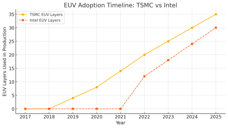
- EUV Adoption Rates:
- TSMC introduced EUV early at N7+, progressively increasing usage at N5/N3.
- Intel struggled with multi-patterning at 10nm before integrating EUV at Intel 4 (2023-24).
- Process Node Implications:
- Intel’s PowerVia integration at 20A/18A requires new tooling and yield management.
- TSMC’s phased approach minimizes risk but may delay competitive performance gains.
✅ Conclusion: Aligning TSMC’s phased roadmap with Intel’s aggressive architectural shifts makes deep process integration unlikely in a JV.
5.2. Interconnect Materials and Wiring
Key Differences in Interconnect Choices
- Intel’s Experimentation with Cobalt Interconnects:
- Used cobalt at 10nm for lower resistance and improved electromigration.
- Later reverted to advanced copper-based interconnects at Intel 4, optimizing with cobalt liner/barriers.
- TSMC’s Copper-Based Approach:
- Stuck with copper but continuously improved barrier materials and low-k dielectric integration.
- Used air gaps selectively to reduce capacitance (RC delays).
✅ Conclusion: Interconnect material differences create further hurdles for a fab-level JV, as both companies optimize differently for yield and reliability.
5.3. Lithography & Patterning Methodologies
Intel vs. TSMC EUV Integration
- Intel:
- 10nm relied on multi-patterning (quad patterning, self-aligned double patterning, etc.).
- EUV introduced at Intel 4, reducing mask count by ~20% over previous nodes.
- TSMC:
- Started EUV at N7+, expanded to 14 layers at N5 and 25+ layers at N3.
- Uses EUV double patterning for tighter pitches, something Intel has only recently explored.
✅ Conclusion: Intel’s delayed EUV adoption puts it at a disadvantage in matching TSMC’s lithography tuning expertise in a joint process node.
5.4. Advanced Packaging (2.5D and 3D)
- TSMC’s CoWoS / SoIC. CoWoS uses a large silicon interposer to link multiple dies (common in HPC GPUs/TPUs with HBM), while SoIC provides wafer-to-wafer (or chip-on-wafer) 3D stacking with fine-pitch copper-copper bonding [9].
- Intel’s EMIB / Foveros. EMIB embeds small silicon bridges in the substrate for localized high-speed interconnect, and Foveros stacks dies vertically on a base die with TSVs [9].
A packaging JV might explore combining these technologies—e.g., an EMIB-based solution with TSMC’s advanced interposers—yet that would demand sharing sensitive packaging IP. Packaging is more feasible for collaboration than core transistor R&D, but it still involves significant proprietary know-how.
6. Financial and Market Impact Analysis
6.1. Financial Projections Under Different JV Structures
Scenario A (TSMC-Run Intel Fab).
A newly formed entity operating a single advanced fab (e.g., ~20,000 wafers/month) might yield ~$2–3 billion in annual revenue if fully utilized, given leading-edge wafer costs often approach $10,000 per wafer [1]. Capex and operational costs, however, would be enormous ($10–15+ billion to build/equip an advanced fab). Government CHIPS Act subsidies could mitigate some of these costs. Over time, if TSMC’s know-how boosts yields, the JV could turn profitable, but near-term margins might be thin.Scenario B (Licensing).
Intel would pay large one-time licensing fees plus ongoing royalties per wafer to TSMC. Intel might save on its own R&D, but face lower margins on the resulting products. From TSMC’s viewpoint, this is “money for IP” with limited investment, yet also the risk of enabling a competitor.Scenario C (Joint R&D).
Sharing R&D expenses (potentially $5 billion or more for a new node) could reduce each firm’s outlay to ~$2–2.5 billion. However, if both produce the same node afterward, differentiation and premium pricing could erode. Past alliances (e.g., IBM-Samsung-GF) show how easily they unravel if one partner alters its roadmap [7].Scenario D (Packaging JV).
Advanced packaging revenues are smaller than leading-edge wafer revenues but growing quickly (driven by AI accelerators, HPC, etc.). A joint facility might reach hundreds of millions to $1 billion+ in annual revenue, with a similarly high capital investment. It could become profitable more rapidly if demand remains strong and if it locks in major customers needing 2.5D/3D packaging capacity [9].
6.2. Competitive Impact on Samsung, GlobalFoundries, and Others
A TSMC–Intel JV would likely consolidate more advanced capacity and know-how under one umbrella, challenging Samsung Foundry (the current #2 in leading-edge) [1]. Samsung might respond by further accelerating its GAA roadmap or emphasizing that it remains an independent alternative for fabless customers wary of working with an Intel-affiliated foundry. GlobalFoundries, having exited the bleeding edge (7 nm and beyond), would be impacted less directly, but might benefit in mature-node niches as TSMC/Intel focus on advanced technology.
6.3. Lessons from Past Semiconductor Joint Ventures
- IBM–Samsung–GlobalFoundries (Common Platform). Shared R&D succeeded until 14 nm but collapsed before 7 nm, with IBM suing GF over abandonment [7]. The risk of diverging priorities is high when large sums must be invested at each new node.
- IBM–Sony–Toshiba (Cell Processor). A one-generation success (PlayStation 3) that dissolved when partners’ needs changed.
- Intel–Micron (IM Flash). Produced NAND competitively for a time, but Intel and Micron parted ways once strategies diverged.
History shows that unless both parties remain fully aligned in technology goals and continue investing at each node, alliances often fail. For Intel and TSMC, direct competition in leading-edge logic poses an even greater hurdle than these past examples.
7. Conclusion
A potential TSMC–Intel joint venture must overcome immense technical complexity, cultural differences, and strategic misalignment.
- Most Feasible Collaboration: Advanced packaging (Scenario D) presents fewer pitfalls, since it avoids direct duplication of core transistor IP. Even so, both sides would worry about preserving proprietary packaging innovations.
- Least Feasible Collaboration: Deep process integration—such as TSMC running an Intel fab or Intel licensing TSMC’s latest node—faces daunting challenges in porting recipes, materials, lithography steps, and design flows. A co-developed process node (Scenario C) is theoretically attractive for cost-sharing but would demand an unprecedented level of trust between two fierce competitors.
- Stakeholder Positions:
- TSMC/Taiwan remains highly protective of its “silicon shield” and advanced IP.
- Intel seeks to regain leadership but fears losing autonomy.
- The U.S. government welcomes more advanced chipmaking onshore but will impose national security restrictions.
- China views any TSMC–Intel alliance in the U.S. as further “containment” of its semiconductor ambitions.
- Broadcom Factor: Rumors of Broadcom’s interest in Intel’s design teams could portend a partial breakup of Intel, with TSMC potentially taking over manufacturing. This underscores Intel’s vulnerability if it cannot execute a turnaround alone.
Technically, Intel and TSMC each bring unique strengths—Intel’s potential leap with RibbonFET and backside power, TSMC’s proven EUV execution and packaging ecosystem. Financially, a well-structured JV might share risk and attract U.S. subsidies, but only if it secures enough demand. Historically, major semiconductor JVs often unravel when partners’ roadmaps or investments diverge.
In summary, while a TSMC–Intel partnership could accelerate technology deployment and build domestic chip capacity in the U.S., it remains a highly complex and uncertain proposition. Packaging or limited one-off collaborations appear more realistic than a full-scale joint fab or shared process node—yet these limited forms still require deft handling of competitive tensions and IP protections. The evolving landscape, including potential carve-up bids from companies like Broadcom, will determine whether TSMC and Intel ultimately come together or continue on parallel, occasionally intersecting paths in their quest for semiconductor leadership.
8. References
[1] Tom’s Hardware (multiple articles). Various reports discussing TSMC–Intel JV rumors and implications.
[2] Semiconductor Digest (multiple articles). Coverage of Intel’s use of cobalt interconnects, reversion to copper, and EUV adoption.
[3] AnandTech. Analyses of TSMC’s EUV integration starting with N7+ and advanced multi-patterning at N5/N3.
[4] Markets.BusinessInsider.com. Commentary on Intel’s IDM 2.0 strategy, analyst views on Intel potentially exiting the foundry business.
[5] Taipei Times. Articles on Taiwanese concerns about U.S. pressure on TSMC and risks of technology leakage.
[6] Reddit.com. Industry analyst discussions expressing skepticism over TSMC licensing its leading-edge process technology to Intel.
[7] DataCenterDynamics.com. Reports on IBM suing GlobalFoundries over the abandonment of 7 nm R&D from the IBM–Samsung–GF alliance.
[8] DigiTimes.com. Reports on TSMC’s collaboration with Amkor for advanced packaging facilities in Arizona.
[9] TrendForce.com. Studies and market data on TSMC’s CoWoS, SoIC, Intel’s EMIB, Foveros, and broader 2.5D/3D packaging ecosystems.
[10] Investopedia.com. Coverage of Pat Gelsinger’s departure in late 2024 amid Intel’s manufacturing struggles.
[11] Reuters.com. White House and U.S. official statements on foreign operation of Intel’s fabs and broader national security considerations.
[12] Forums.Anandtech.com. Technical deep dives and comparisons of Intel’s vs. TSMC’s standard cell heights, transistor density, etc.
[13] SemiWiki.com. Analysis of TSMC’s EUV adoption timeline and multi-patterning transitions at advanced nodes.